If you've built a few projects on breadboards or maybe even on solderable prototype boards, like an ElectroCookie, you may be wondering when it is time to consider designing your own printed circuit board or PCB. Maybe you think it is too complicated or too expensive? Well, in this article, I'm going to cover my journey of creating my first PCB, using it in my project and also cover what I learned and what I might do different the next time.
First off, this is not going to be a step-by-step, how-to process of designing a printed circuit board. I'll cover the major steps that I used (and may do a live stream later that covers much of the step-by-step), but is more about giving you a general idea of the process and actually how simple it really was. As always, there is a YouTube video of this process if you prefer to watch instead of read.
Next, this PCB is really the second part of a project that I built in the previous article that covered the use of port expanders for ESP boards (you can watch a YouTube video of that project). In that article and video, the final build was an analog-style LED clock, with over 72 digital I/O pins from a single ESP8266:
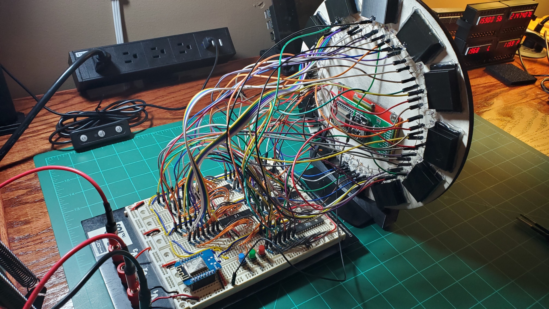
But this was built entirely on a breadboard, with literally hundreds of wires:
As I mentioned in the previous article and video, this is not the most efficient or even the best way to build a clock. The original intent was to demonstrate the use of I/O port expander by controlling 72 individual LEDs.
But once it was done, I liked some of the features that were built into the clock. Keeping it in the breadboard state however, was simply impractical. This is what finally pushed me to explore what was involved and what the costs would be to design a custom PCB. I had never even messed around with any PCB design software before, so I was a true beginner. And this is where my journey starts.
Parts List
Most of these parts are covered in the related article on Adding I/O pins to your ESP, but this PCB version does have some different parts. So, I'll list all the parts that I used for this build. You might find different quantities or better prices elsewhere, but these are the actual items I ordered and used in my project.
Some of these links may be Amazon affiliate links. Use of these links will not affect your pricing, but as an Amazon affiliate this blog may earn a small commission if you make a purchase.
3D printed Parts
For most of my projects, I try to design them so that even if I use 3D printed parts, they aren't required and often alternatives can be found. This project is an exception. The 3D printed parts are likely required if you want to build the PCB and clock as I have. The original breadboard version used a premade wooden clock face, but because the alignment of the LED mounting holes on the PCB need to line up precisely with the faceplate, manually drilling countersunk holes in a wood panel would probably not be accurate enough. So for this project, I designed and 3D printed the following parts:
- Clock face
- Number covers (for the hour number cutouts)
- Standoff mounting blocks
- Clock stand
- ILI9341 display trim
There are copies of the .stl files for these parts in the Github repo.
Software Used (free)
All the software used in this project is free. Some is web based, while others have both a web and local downloadable version. I won't be covering the details on how to use this software here, but ample information is available online.
Clock Face 3D Design: Fusion 360 (version for personal use is free)
*The code for the clock was developed using v1.8.16 of the IDE as some libraries still have not been updated to work correctly with the new 2.x version. If you run into compile errors with v2.x, try using v1.8 of the IDE. Both can be installed side-by-side.
Designing the PCB
Since this was my very first PCB, there was a bit of a learning curve... not only with the design tool, but also with some of the terminology. Things like vias, ratlines and net ports were all new terms for me and took a while to understand their meanings. And while I'm using EasyEDA, there may be some differences in particular steps if using other software. But the general steps will likely be the same.
While there is simply too much material to cover here in a single blog article to describe each individual step of the process, I will cover the major steps and a few details that might help you get started. In addition, in the Github repo you will find JSON files for both my schematic and PCB design. You can import these into your own copy of EasyEDA and explore in more detail how I created my version.
Before beginning any PCB design, you should first have a working breadboard version of your project. This assures that the wiring and logic are correct and you can also use the breadboard design to help with the PCB layout.
Create a Schematic
 |
| Click to enlarge |
The first step in creating a schematic is to simply place all your components on the workspace. There is a library search option, and odds are that you will find nearly any component you might be using. In fact, you will often find many copies. Check different versions to find the one that matches the component you will be using. Remember to include any pin headers, connectors or other components that might be part of your breadboard. Basically, you want everything except the actual wiring runs from the breadboard version included in your schematic. The physical layout here is not important and has nothing to do with the actual PCB design. You want the schematic to be readable and easy to follow as to how the components are connected.
 |
| Click to enlarge |
Once all the components are in place, you then have to "wire" them together to show how they are connected. For simply circuits, using the wiring tool as shown above is probably fine. For more complex designs with a lot of pins connected together or to a common point (like your voltage or ground) and where the resulting wiring would be like spaghetti and hard to read, using something called 'netports' can greatly simplify the diagram.
 |
| Click to enlarge |
When you add netports and give them a name, all netports with the same name will automatically be connected together when converted to a PCB. What's more, if you create a copper pour area, like a ground plane and give it the same name as the ground netports (e.g. GND) then all the ground connections will be automatically connected to this copper area and you won't have to create any traces!
 |
| Click to enlarge |
In many cases, you may use a combination of wiring and netports, as I have done above. The resistors and LEDs are connected with wiring, but all the ground connections and other common connections for the port expander use netports. Also note the green "X"s on some of the pins above? If any of your components have pins or connections that will not be used, you need to indicate that by applying the 'not connected' flag on them. All pins and connections must have either a connection or a 'not connected' flag or you will get design errors when creating the PCB.
Once you have the schematic created and all connections established, it is time to create a PCB design from this schematic. In EasyEDA, a menu option allows you to convert your schematic to a PCB. That's the next step.
Laying out the PCB and Traces
 |
| Click to enlarge |
When the PCB is first generated, you will be asked for the size and shape of the board. By default, this will be a basic rectangle, but you can change both the shape and size. For my clock, I needed circle just slightly smaller than the planned faceplate size (which was determined by the maximum build size of my 3D printer). Also by default, your board will have two "layers" were tracing (or wiring between components can be run). There will be other layers listed for things like silk screen, paste masks, etc.
The top and bottom layer are, by default, copper layers. Components will normally be placed on the top layer (but they can be placed on the bottom if needed) but your traces can use either layer. For more complex boards, you can add additional copper layers, but this does come with an additional cost, so you should only add them if necessary. I ended up with four copper layers in my board.
In the lower corner are all the components you defined in the schematic. All those blue lines? Those are called 'ratlines'. They are not the traces for the PCB but instead show you all the connections.. or traces... that will need to be made between your components.
Now you begin the process of placing your components on the PCB. You will likely adjust positions multiple times during the tracing, but there are tools to help you with positioning, rotating of components, etc. When placing components, you need to try to keep the traces in mind, to both simplify and to try to create a design that will only utilize the two default copper layers.
Quick tip: If you have already drawn a ground plane or copper area and then move a component that had a ground connection, it will leave "gaps" in the copper. Or if you try to draw a trace through the copper area, it will initially show as invalid:
Simply select the ground plane or copper area, right click and choose the option to rebuild the copper area.
Not only will this "patch" the gaps left behind, it will also carve out an area around your traces, making them valid. This took one of my great YouTube subscribers, @Cowfeet1, to show me this little trick... and it would have saved me significant time if I had known this from the start.
You will also need to take into account assembly of the components onto the PCB after you receive it. if you place components too close together you may have problems trying to solder those parts. You also need to add any mounting holes or other needs you may have as part of your project's final assembly.
And of course traces cannot 'cross' each other. If you are in a position where a trace needs to cross another, this is where 'vias' come into play. Vias allow you to route your trace to another copper layer and, in effect, jump over another trace on a different layer.
Have you ever looked at a circuit board and noticed all those little holes that don't seem to be connected to anything? Those are vias. So, by placing your components carefully, sometime changing their orientation and by making use of vias, you have to connect all your components and replace those ratlines with copper traces. It can be a time-consuming process... but I personally found it challenging and a bit like trying to solve a line maze. "Nope... dead end going that direction. Maybe if I rotate the component, I can route the trace here instead."
If you really do get to the point where there doesn't seem to be any valid path to create a trace, that's when you can add an additional copper layer or two. You now have three or four different layers where you can route your traces.
There are tools that will try to 'auto-trace' your PCB for you. They can be successful sometimes, but the more complex your board, the more likely they will be unable to auto-route your board.
 |
| My final PCB Design - Click to enlarge |
If you look closely at my final design above, you'll see traces in red, which are on the top layer and other traces that are grayish. Those traces are on a different layer which is why they can "cross" the red traces on the top layer. My board also has a full ground plan as the bottom layer. This means all of my ground connections (those that had an original net port of GND... the same as the port of the ground layer) were connected automatically and I didn't have to create traces for any of those. The green area in the center is also on a middle copper layer and is a 3.3V plane. All 3.3V connections for the components automatically route and connect to this plane on a middle layer.
Once you think you have a successful design, you can run a "Design Rule Check" (DRC) from the menu. This will verify that you have complete all required connections and also that you haven't violated any design rules... like running a trace too close to a component pad. If there are any errors, it will be pointed out and you'll need to fix the errors. But once you are error-free, you are ready to create the file to send off for manufacturing. This is called a Gerber file and can be created via the menu. Save this Gerber file (actually a .zip file) and you are ready to place your order.
Ordering, Cost and Delivery
Once you have your Gerber file, you can upload it to a number of different PCB manufacturer web sites to have your PCB made. In fact, I tried a couple of different sites just to compare costs and delivery times. I settled on using JLCPCB because they simply had the better price and an estimated 1-2 week delivery time. But PCBWay is another popular options and there are others. I recommended trying a few different sites to compare costs and delivery times.
For JLCPCB, I simply uploaded my Gerber file to get started and get a cost.
 |
| Click to enlarge |
As you can see, just from the Gerber file, the size, number of layers and all information for creating the PCB are loaded. There are a ton of different options that you can specify, such as the PCB and silkscreen colors, along with many options for special needs. I just accepted all the defaults for my board and didn't change anything. There is a minimum quantity of 5 for any orders. Naturally, the cost per board goes down with higher quantities, but you can experiment with different values on this same page.
Once satisfied with your order, you can add it your cart and move to the check-out. Note that each submitted order will go through an internal review process for errors or issues before it is accepted. You have the option to go ahead and enter payment information or wait until final approval. If there are any issues or questions, you will be notified.
In my case, my board was approved and accepted in about 15 minutes at which point I entered my payment information and manufacturing started!
The web site will actually track and show you each step of the manufacturing process... I thought this was kind of slick to follow along since it was my first board. They also have videos that show you what occurs for each step. Nice!
And despite my order sitting in shipping for a couple of days, I received it exactly one week after I placed my order. That's pretty amazing (to me anyway) that the board could be made and shipped from Hong Kong, arriving in Indiana only a week later! And I could have received it even sooner if I wanted to pay for expedited manufacturing and shipping.
The PCBs were vacuum sealed and packaged very well, with plenty of bubble wrap padding.
The silkscreen was all nicely done and everything was clearly readable. All-in-all, I was very happy with JLCPCB, the order process, delivery time and quality of the boards.
Assembling The Project (and what I learned)
Mounting the components to the board, designing the 3D printed face and assembling the final project is something that is much better viewed via video than me trying to describe it here in a written blog. So if you want to see more about those steps, please watch the YouTube video. I'll only cover a few items here.
I decided to use sockets for my port expanders instead of soldering them directly to the PCB. That would make replacement quite a bit easier should one of the MCP23017 chips fail or overheat.
I also decided to mount the Wemos D1 Mini on pin headers as well. This would facilitate replacing it if necessary, or as shown as above, even upgrading to an ESP32 Mini... since the inner row of pins on the ESP32 Mini are compatible with the D1 Mini (5V, 3.3V and GND... other GPIO pins would have to be updated in the clock controller Arduino code).
The clock face was 3D printed and designed using Fusion 360. The clock face needed to be designed so that the holes for the LEDs lined up precisely with the mounting holes on the PCB. This is why I replaced the original wood clock face with a 3D printed version. Using the PCB design and Fusion 360, it was easy to get this precise alignment.
What's more, each LED hole is slightly countersunk so that the LEDs will all slightly protrude the same distance from the front face of the clock.
I didn't feel it would be possible for me to do this with a hand drill and a wooden face plate. The one drawback is that I was limited on maximum size of the faceplate (and therefore the PCB) based on my 3D printer.
The maximum print size for my 3D printer is 220 mm x 220 mm and the clock face diameter was 215 mm. So even after disabling/removing the normal skirt that I have on other prints, this barely fit with only 2.5 mm of spare printable area on each side.
Overall, I was pretty satisfied with the 3D printed version on the left as compared to the original breadboard wooden clock face on the right. The number are a bit smaller due to the larger diameter ring of the minute LEDS but I feared that moving the LEDs closer to the center was going to make installation between the PCB and face plate even more difficult.
As you can see, it was a bit of an adventure getting the LEDs between the two. Again, you can see more detail on how I did this in the video. But in the end, it worked out pretty well.
Is it perfect? No... but for a first attempt at creating a PCB, it turned out much better than I expected. And more importantly, everything was designed correctly with the PCB. But there are a few things I'd do differently. Some I can do with one of my extra PCBs... others would require designing a new PCB.
What I Would Do Different (Version 2)
There are a few things I am going to improve with version 2, which I can create on one of my extra PCBs. And then I can just swap out the new PCB for the old one with the same face plate. This is where it was fortuitous that I socketed the MCP23017 port expanders and the D1 Mini. I can simply transfer those to the new PCB and won't need to purchase new ones.
Use Larger Value Resistors for Minute LEDs
The minute LEDs are bright. Really bright. Too bright! When looking straight on at the clock when about 20 or more of the LEDs are on almost hurts the eyes! And when nearly all the LEDs are on? I think you could read a book in a completely dark room with just the light from the clock!
Originally, I selected 180Ω resistors for the minute LEDs. This value was selected more for limiting the maximum current through the port expanders and not the brightness of the LED. For the replacement PCB, I will up these resistors to 220kΩ... a significant increase! But I did some breadboard testing and I think this will dim the LEDs enough to not be blindingly bright, but still bright enough to see the time from across the room.
Diffusers on hour LED openings
For the green hour LEDs, I only used 75Ω resistors. Normally the brightness here isn't an issue, but when the light shines directly through an opening it can still shine right in your eye. Also because of the somewhat directional nature of the LEDs, some of the numbers really don't evenly light up. You can tell the hour by the position on the clock, but often you really can't "read" the number. I'm going to try adding some sort of thin diffusing material on the back side of each number to try to get a more even glow for the numbers. I'm unsure of the material at this point. It could be as thin as just a small square of paper or at thick as the Styrofoam paper plates I used on my Hexagonal LED Wall Display. I'll experiment with different materials.
There are some additional changes I'd make, but these would require making changes to the actual design of the PCB (and ordering new ones).
Relocate push buttons to allow wall mounting
My original hope was that I'd be able to create some sort of wall mounting bracket that would let me hand the clock on the wall. I didn't remember this when I designed the location of the push buttons! If the clock was hung on the wall, the buttons would become inaccessible without removing the clock from the wall. If redesigned, I'd change the orientation and move the buttons more to the side. In fact, I'd probably just use pin headers on the PCB and move the buttons to the clock face, connecting them to the PCB with standard wiring.
Move 5V Barrel Jack
Since the clock couldn't be hung on the wall, I 3D printed a simple desk stand for it, as you can see in the above photo. But the placement of the barrel jack for the 5V power connection caused issues for using the clock on the desk.
Both the location and angle made it impossible to connect the barrel connector from the power supply without either rotating the clock (so that 12 o'clock was no longer at the top) or raising it up higher. I had to order a 90° barrel jack adapter to be able to connect the power. If the clock were to remain on the desk, I'd reorient this connection. Or if I knew that I was going to move the buttons and really hang it on the wall, I'd probably move the barrel jack to the bottom edge of the PCB.
Larger 5V trace
One of my YouTube subscribers was reviewing my PCB design and noted that my main 5V PCB trace might be too small to adequately carry the current needed by the clock, LEDs and the ILI9341 touch screen display. At the time, I didn't know anything about trace size and that I could make the trace larger for higher current.
Out of an abundance of caution, I opted to add wire leads directly from the barrel jack for powering the ILI9341, thereby bypassing carrying this current through the PCB trace. If I redesigned the PCB, I'd increase the size of the 5V traces so I could power the ILI9341 off of the PCB pins that I originally designed for that purpose.
Consider the Assembly Process and Controller Coding
When I was designing the original PCB, I was focused solely on the electronics and components. I wasn't really thinking about either the assembly or the code to make it all work. For example, the through holes in the PCB for the standoffs aren't consistent or at any particular location. I just dropped them in wherever I felt that they fit best. This made it much more difficult on the 3D printed face plate design, because the location for the standoffs could not be precisely determined from the PCB design (unlike the LEDs... which were in very precise locations).
Also, the code for controlling the LEDs would have been greatly simplified if the wiring for the LEDs in the PCB were simply shifted by one position counter-clockwise. This would be very easy to accomplish in the design of the PCB and would not have been any real extra work when laying out the traces. But I wasn't considering the code when laying out the PCB LED locations.
Both of the above items would be very easy to correct if designing the PCB again.
UPDATE: Version 2 Changes and Results
After this article was originally published, I did take one of the extra PCBs and rebuilt the system, making two of the changes listed above... plus adding one more.
First, I used 2.2 kΩ resistors instead of the original 180 Ω resistors for the minute LEDs. This was major improvement as the LEDs aren't blindingly bright, but still adequate. However, with the dimmer LEDs, the difference in the red LEDs and the yellow LEDs at each five minute mark isn't as distinct. If there is ever a version 3, I'd probably use green LEDs instead of yellow at the 5 minute marks so they are a little more distinct.
Next, I added diffusers to the bottoms of the number cover blocks. These are simply small squares of paper (just slightly heavier than standard printer paper... these were from a block of Post-It style notes) that are glued to the back and will rest directly against the back side of the clock.
This greatly enhanced the readability of the numbers as the light is now diffused throughout the entire number cut out instead of being bright hotspots. The dimmer minute LEDs are also shown above, which also helps the hour number to stand out.
Finally, if you look at the photo of the diffusers on the back of the number covers above, you will see a short 6" micro USB to USB A cable has been attached to the ILI9341.
This hangs out the back of the clock and provides a way to re-flash the ILI9341 without disassembling the clock should it ever be necessary due to an issue where it could not be flashed over the air (like a corrupt flash or runaway code... which I did once, which is why I wanted this cable available for the future).
I doubt that I will make any additional changes to the clock at this point. Any other upgrades or improvements would likely require a new, updated PCB design.
Will I Design a PCB Again?
 |
| A WLED controller board - with lots of breakouts for peripherals! |
Absolutely! In fact, I've already designed two additional PCBs for other projects since I finished the clock. The entire process was much easier and not as expensive as I had originally believed. And as I mentioned above, I find the process of designing the boards and trying to figure out all the route tracing to be both challenging and entertaining. If I have a simple one-off circuit needed for a project, I'll probably stick with my ElectroCookie solderable prototype boards. But for anything more complex or situations where I might build or use more than one, then it will be custom PCBs for me for the future!
Additional Project Information (for those that are interested)
The following information really has nothing to do with the PCB itself, but is really more a functionality of the code and the ESP8266 clock controller. But I'm including it here for anyone that might have interest in how the final clock project actually works. Note that any photos shown in this section were prior to the enhancements made in version 2 as described above, such as the number diffusers.
The Code
The clock code, designed for the Wemos D1 Mini (but should run fine on any standard ESP8266 board), is Arduino/C++. Currently, it requires the Arduino IDE (or compatible IDE) to compile and install the code. WiFi and MQTT information, along with other settings and options are specified in include .h files. The code has substantial documentation within the code itself, and more information can be found in the Github repo and related wiki.
It would be relatively minor to modify the code for an ESP32 (primarily swapping out some libraries for the ESP32 version and changing a few GPIO pins to match the ESP32 pin alignment). However, I will not be developing an ESP32 version so if you want to use an ESP32, you will need to clone or fork my code and make those changes yourself.
The ILI9341 display seen in the middle of the clock face actually runs ESPHome on its own ESP32 controller. More details on this are provided below.
Features
For the hours on the clock, each number lights up to indicate the hour (and all other hour LEDS are off). However, the clock has a number of options as to how the minutes are display. There are current five different display modes for showing the minutes (each mode is currently showing the same time, 6:42, in the following examples):
Full Display
In this mode, all the LEDs light up as the minutes increase each hour. A separate option allows you to set whether the LEDs "sweep" each new minute... in other words, redraw all the LEDs in order from minute 1 to the current minute... or to simply light up the next LED in the sequence without redrawing or "sweeping".
Single Minute Display
In this mode, only a single LED will be lit to show the current minute of the hour.
Five Segment Display
In this mode, five LEDs will be lit, with the last LED being the current minute. This five LED segment will travel around the the clock as the hour progresses.
Ten Segment Display
This is similar to the five segment display, except ten LEDs will be used.
Fifteen Segment Display
Like the five minute and ten minute options, this display uses a 15 LED segment to indicate the current minute.
One of the push buttons on the back of the clock allows you to toggle through the different display modes. Of course the mode can also be changed via MQTT/Home Assistant as well, but more on that below.
Blink Current Minute
Each of the display modes has an option to blink the current minute LED off and on at a default cycle of one second. But the cycle length can be changed in the code settings. If turned off, then the LED just remains solid without blinking.
All LEDs On/Off
All LEDs can be turned off or on. The clock continues to operate and keep time while the LEDs are off. This can be done with one of the push buttons or again, via Home Assistant. I used a Home Assistant automation to turn all the LEDs off when the rest of the lights in the room are turned off, so the clock doesn't stay lit all night. This automation also turns off the ILI9341 backlight... but again, more on that below.
OTA Updates
While the first load of the code to the D1 Mini/ESP8266 has to be done via a USB connection, after the first load, all future updates can be done over the air. The OTA update process is described in more detail in the Github repo wiki.
Getting the Current TIme
As currently written, the time is received from Home Assistant via MQTT. At the top of each minute, Home Assistant sends an MQTT message that the clock receives to update its time. This does mean that MQTT is required, along with Home Assistant or another system that can send an MQTT message to the appropriate topic with the correct time. See the Github repo wiki information on MQTT for more details.
It would be relatively minor to add an NTP server to the code and modify it so that the time was received from the Internet (or your own local NTP server). But I will not be making a version that uses anything other than MQTT, so that will be on you if you wish to use a different time source.
Home Assistant Integration via MQTT
As mentioned above, the clock relies on MQTT message to receive the time. I am using Home Assistant both as my MQTT broker and to send those time-based MQTT messages. But the clock also accepts additional commands for controlling most of its features. It also reports back its current state via MQTT. This means that you can integrate the clock into Home Assistant for display/control on a dashboard:
 |
| Click to enlarge |
But in addition to control via dashboard, you can use the clock in your automations. For example, I have the clock turn off all the LEDs (and the ILI9341 display) at night when the room's lights are turned off. See the Github repo wiki for all available MQTT topics and payload formats used by the clock, along with my Home Assistant code for integrating the clock and creating the dashboard shown above.
The ILI9341 Display
The ILI9341 TFT touch screen seen in the center of the clock face is actually independent of the clock itself and isn't even required. The only thing is shares with the clock is the 5V power supply. It can be completely omitted if desired.
However, the ILI9341 runs ESPHome. It also utilizes a special library by 'Dorffmeister' to make the display easy to use. By default, I am showing the current day of the week, the date and indoor and outdoor temperature. All of these values come from Home Assistant sensors. But since it is a touch screen:
A simple touch will toggle the display to show the current 5-day weather forecast. Tapping again will return it to the previous display. While I'm using it for date and weather data, since it is an ESPHome device (and thereby natively integrated into Home Assistant), you can use the display to show whatever information you like, including changing the information based on Home Assistant automations.
You can find more information on using the ILI9341 display with ESPHome in the additional information below, along with a link to Dorffmeister's library.
That's a wrap for this project. Let me know down in the comments if you have any questions not addressed here, in the related video or in the links that follow. And thanks for reading!
Additional Links and Info
Github Repo (Clock code, MQTT info, PCB and 3D design files, etc.)
If you'd like to support future content on this blog and the related YouTube channel, or just say thanks for something that helped you out, you can say thanks by buying me a one-off cup of coffee at:


No comments:
Post a Comment
To help eliminate spam and to keep all conversations civil, submitted comments are moderated. Therefore your post may not show up immediately. Please be patient as most reviews are completed within a few hours.